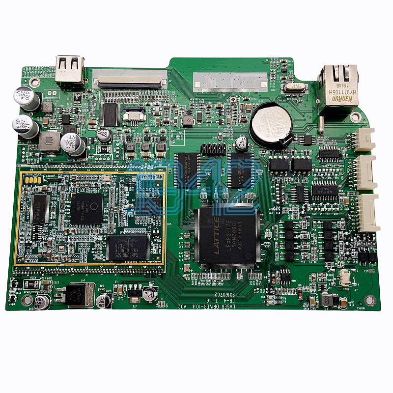
Point:433
Components type:125
PCB size: 186mm*147mm
Minimum package size of resistance capacitance sensing: 0402
Minimum device pin spacing:0.5mm
Welding mode:Reflow soldering for double side+ Wave soldering.
Manufacturing process: PCB producing+components procurement+assembly
Shenzhen 1942 Technology Co., LTD is a professional PCBs manufacturer, 7 SMT production lines ,5000㎡ factory
Main bussiness : PCB design , SMT, DIP, compnents soucing, function test , PCBA coating, PCBA failure analysis.
PCBs applications:
medial equipment PCB& PCBA
industrial control PCB$PCBA
IOT ( internet of things ) PCB &PCBA
drones PCB & PCBA
Video equipment PCB &PCBA
…………
The total number of front and back surface mount components is 433
The amount types are 125
The outer diameter of PCB is 186mm*147mm
The minimum package size of surface mounted components is 0402
The minimum pin spacing of surface mount components is 0.5mm
Components are soldered by double-sided reflow soldering machine & wave soldering oven

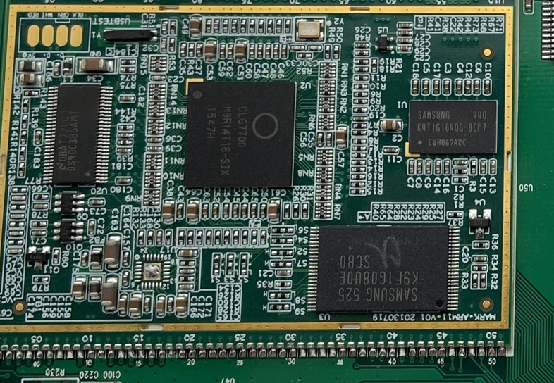
Module mounting

The production technical difficulty of this PCBs is mainly the mounting of modules. It is necessary to ensure that the mounting height of modules is consistent . Furthermore, this module is very easy to be mountedwith false soldering.
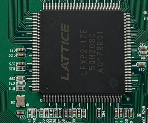
Main chip mounting

The number of pins is large and the spacing is small. The surface mounting process should be very high. At the same time, pay attention to the cleaning of PCBs board

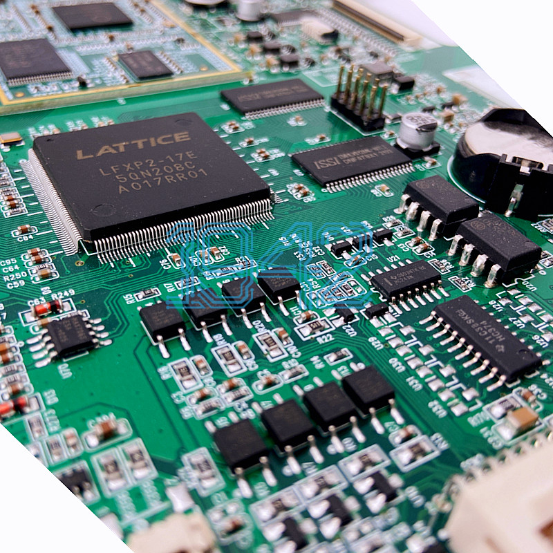
The design and mounting of this Laser marking circuit board are very difficult, because the PCB size is small, but the design is very complex, there are many kinds of materials, and there is a large module, which reflects a high design level and mounting technology
#Shenzhen PCBa manufactuer #PCB factory #1942 PCB assembly manufacturing # SMT factory