

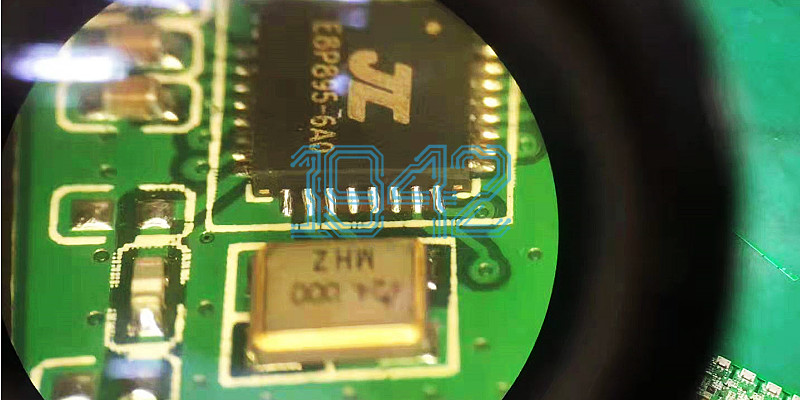
QFN package refers to Quad Flat No-leads Package, which is one of various packages of SMT surface mount components. After SMT processing and soldering, why does the pad around the side of QFN not receive solder paste or the solder paste spreading height cannot meet the customer's requirements? This is a long-term painful problem for SMT personnel. Next, Shenzhen 1942 Technology Co., LTD ,one stop PCBA supplier will share with you why it is difficult to solder QFN? How to solve this problem? Hope this article will bring you some help!
Due to the preciseness of SMT processing technology, many SMT practitioners believe that the solder paste spreading of the QFN side pad should be as full as that of the QFP pin ,then the soldering is normal, while the exposed copper on the QFN side is not covered by solder, which means that the soldering is abnormal. In fact, this is not correct. Whether the solder paste coating on the QFN is abnormal or not is mainly determined by the bottom soldering effect. As for the amount of solder paste spreading on the side, it is generally subject to the customer's requirements. According to IPC-A-610 standard, the solder spreading degree of QFN side pad is divided into three grades; Level 1: the bottom of QFN pad is obviously wetted with solder paste; Level 2 is 25% of the height of the side pad; Level 3 standard is 50% of the side pad height;
1、 Why It Is Difficult To Spread The Solder Paste When Solder The QFN Chips
As the ends of the side pins of QFN are all bare copper, and the chemical reaction of copper in the air 2Cu+O2=2CuO produces copper oxide. As we all know, there is a similar PCB called "bare copper PCB", which is easy to be affected by acid and humidity and cannot be kept for a long time. It needs to be used up within 4 hours after unpacking, otherwise the copper exposed in the air will be oxidized, which will affect the PCBA soldering quality. Similarly, if the solder paste spreading on side tin of QFN must be required, the time after the cut section of QFN is exposed to copper must be controlled. Since the transportation and storage time between QFN manufacturing and SMT processing is much longer than 4 hours, it is unrealistic to achieve good solder paste spreading effect. The real reason why the side of QFN side pin is not easy to solder is that the side pin of QFN is cut, and there is no soldering treatment on the surface after cutting, so there is an oxide surface.
2、 Solutions
1) The Stencil opening mode can be internal cutting and external pulling, it can be properly adopted to reduce the cross cutting size of the pad position by internal cutting, and reduce the occurrence of bad conditions such as tin bonding and bridging during soldering. At the same time, the stencil opening at the QFN chip pad position is extended to increase the amount of solder paste at the QFN pin to ensure that there is enough solder paste in the spreading process;
2) Select the lead-free environmental protection technology QFN special solder paste. Select SAC305 or SACX0307 high temperature QFN solder paste, and choose No. 4 powder. During stencil printing, give more solder paste, which is helpful for tin climbing;
3. Before PCBA enters the reflow soldering oven add a proper amount of solder paste around the QFN pad, and the soldering effect will be significantly improved.
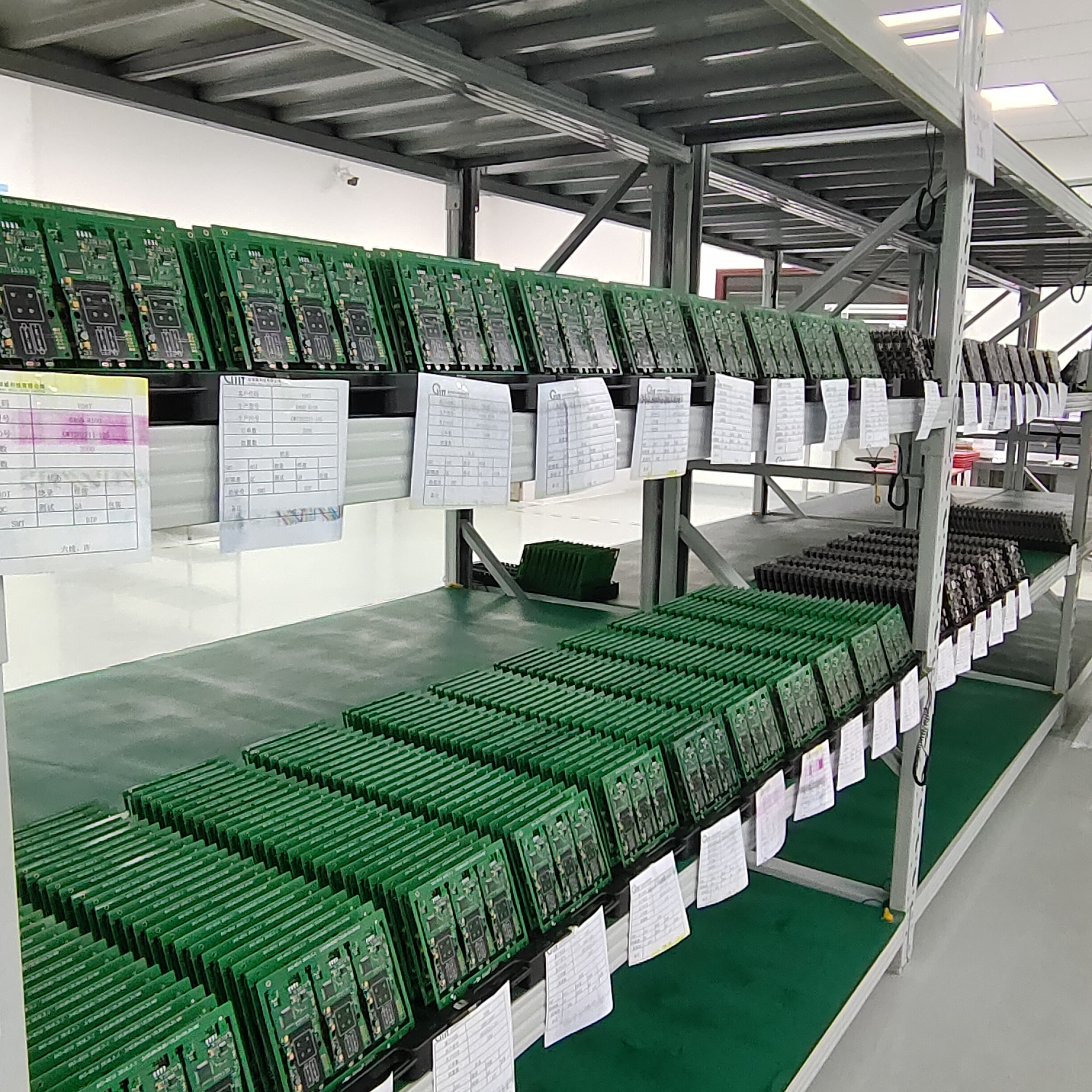
For more information about PCB and PCBA, please visit www.pcbasz.com, or send your Gerber and BOM for detailed quotation.
 2024-06-03