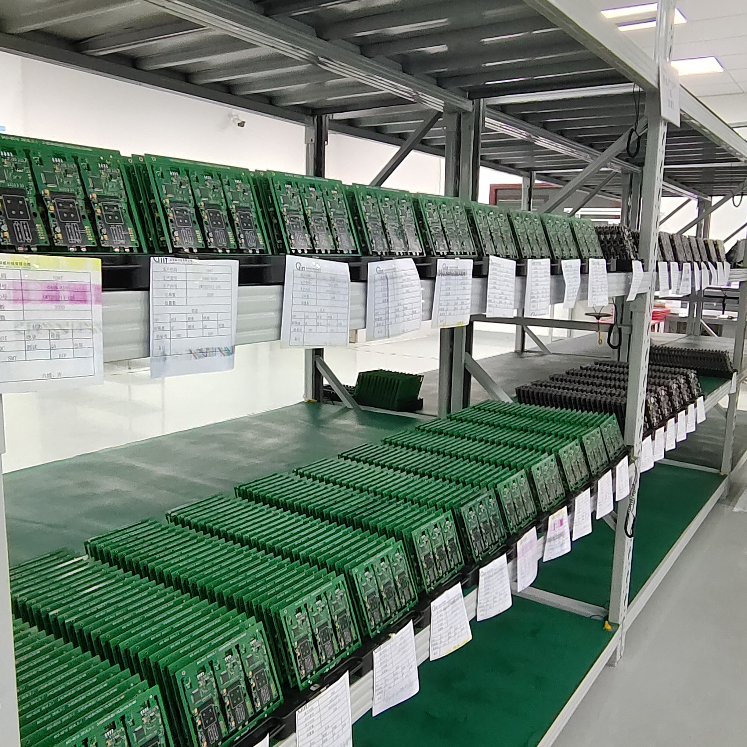


Solder paste explosion means when assemble the components, solder paste bursts and ejects at the junction of PCB solder joints and the solder paste. This phenomenon generally occurs during PCBA wave soldering. Solder paste explosion in PCB Assembly will lead to defects of PCBA solder joints, and it is also the main reason for the formation of solder beads on the surface of PCBs. What are the reasons for explosion during PCB Assembly? How to solve this problem? Next, One stop PCBA supplier, Shenzhen 1942 Technology Co., Ltd. will share some suggestions with you
1 Cause analysis of solder paste explosion during PCB assembly
- The main reasons for solder paste explosion are generally that PCB, solder paste and components are affected with moisture or wave soldering fixture is affected with moisture. If all soldering materials and auxiliary materials are exposed to the air for a long time and absorb too much water, the explosion will occur at high temperatures.
- In addition to the first point, the nonstandard use or incomplete volatilization of flux during PCB assembly is also the main reason for solder paste explosion. For example, the amount of flux is too much, the flux is damp, or the composition proportion of the flux has problems.
- The fixture used for wave soldering of PCBs has too many impurities, and the solder paste inside the wave soldering furnace contains too many impurities.
- The size of PCB through-hole does not match the size of component pins, which is often ignored by many PCB assembly factory and industry professionals. When the PCB is going through wave soldering, the solder paste surges up from the bottom of the PCB, if the pin of the component does not match the hole position, a large amount of hot gas will exist in the through-hole and will not be dispersed, thus forming explosion. Combined with the dampness phenomenon in point 1, the probability of explosion will be greater and the situation will be more serious.
2 Solution to solder paste explosion
- According to the PCB baking conditions: 120 ℃-4 hours, if the PCB is a paper based plate, setting 60 ℃-8 hours. If the PCB after SMT mounting for more than 48 hours undergoes wave soldering and explosion occurs, the PCB is likely to absorb water again. Experiments have proved that this phenomenon can be solved quickly. Set the SMT reflow soldering temperature to [80 100 100 120 130 140 160 160 160 160 ℃] and the chain speed to 0.75 m/min, and then process the plug-in after the second reflow soldering. This phenomenon is the fastest and most effective way to solve the problem of tin explosion in PCB assembly.
- Check whether the flux is used too much, reduce the amount of flux used, control the amount of flux according to the range of 25ml/min to 40ml/min, and test whether the actual temperature of PCB surface in the actual preheating area reaches 115 ℃ to ensure that the flux is completely volatilized.
- If explosion occurs only in the assembly process of a batch of recently produced PCBA, and soldering explosion occurs under other unchanged circumstances, it is necessary to consider that PCB costing and flux are not equipped, and a flux from a different supplier can be used.
- In PCBA soldering processing, if there is fixed solder paste explosion on the PCB surface, it is easy for technicians of PCBA factory to ignore the problem of detecting whether the PCB hole position matches the component pin. Refer to the following list.
|
Pin Diameter(D) |
PCB through hole inner diameter |
|
D<=40mil ( 1mm) |
D+12mil |
|
40mil<D<+80mil |
D+16mil |
|
D>80mil |
D+20mil |
 2024-06-03