

Optimizing PCBA New Product Introduction (NPI): A Guide to Accelerating Hardware Time-to-Market
In the electronic hardware industry, transitioning a design from the engineering lab to mass production is often the most critical phase of a product's lifecycle. New Product Introduction (NPI) in Printed Circuit Board Assembly (PCBA) requires more than just standard manufacturing; it demands a specialized approach to identify design flaws early, optimize manufacturing efficiency, and mitigate supply chain risks.
For hardware startups and enterprise R&D teams alike, partnering with an agile, NPI-focused PCBA manufacturer is the key to securing a competitive market advantage.
The Strategic Role of NPI in PCBA Manufacturing
Traditional contract manufacturers (CMs) are optimized for high-volume, low-mix production. When handling prototypes or complex, low-volume initial runs, their workflows often lack the flexibility needed to address design ambiguities.
An expert PCBA NPI service bridges this gap by treating the first production runs as an extension of the engineering process. Rather than blindly assembling components based on provided files, NPI specialists actively scrutinize the technical package to guarantee seamless scalability.

1. Advanced DFM (Design for Manufacturability) Analysis
Before a single board enters the SMT (Surface Mount Technology) line, a thorough DFM review is essential. This technical evaluation prevents costly re-spins by identifying critical layout issues, such as:
- Component Footprint Mismatches: Verifying that land patterns precisely match component data sheets to avoid soldering defects like tombstoning.
- Thermal Relief Optimization: Ensuring appropriate trace and plane connections to prevent cold solder joints during reflow.
- Via-in-Pad Interferences: Detecting un-capped or un-filled vias that can cause solder migration away from critical component pads.
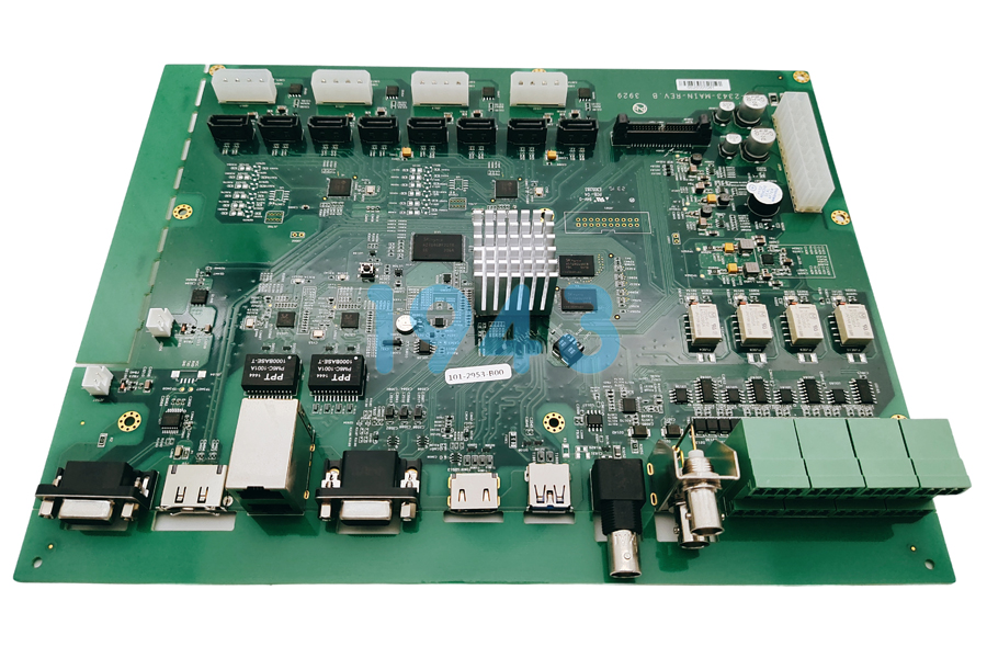
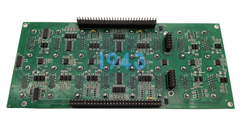
2. SMT Precision for Complex Hardware
Modern electronic hardware increasingly relies on high-density, fine-pitch components such as BGAs (Ball Grid Arrays), QFNs, and 0201/01005 passives. Successfully assembling these components during an NPI run requires stringent process controls:
- Solder Paste Printing Accuracy: Utilizing precision laser-cut stencils and 3D SPI (Solder Paste Inspection) to ensure consistent paste volume deposit.
- Reflow Profile Customization: Developing bespoke thermal profiles based on the board’s mass and component density, ensuring reliable intermetallic joints without thermal stress.

Streamlining the Supply Chain: Component Sourcing & Risk Mitigation
Hardware development timelines are highly sensitive to component availability. A specialized NPI service minimizes these bottlenecks through proactive supply chain management.
| NPI Supply Chain Strategy | Technical Benefit | Impact on Time-to-Market |
| BOM Lifecycle Scrutiny | Identifies End-of-Life (EOL) or Obsolete parts before production begins. | Prevents last-minute re-designs during active production. |
| Alternative Component Validation | Cross-references secondary, drop-in replacement parts for high-risk components. | Eliminates long lead-time delays caused by sudden market shortages. |
| Authorized Procurement Only | Sources components strictly from franchised distributors to eliminate counterfeit risks. | Ensures electrical performance and reliability meet strict engineering standards. |
Structural Quality Assurance and Testing Protocols
To guarantee that an NPI run yields functional, field-ready hardware, a multi-tiered inspection and testing framework must be integrated into the PCBA process.
- Automated Optical Inspection (AOI): Deployed pre-reflow and post-reflow to verify component placement, orientation, and polarity with high throughput.
- X-Ray Inspection (AXI): Crucial for hidden solder joints beneath BGAs and QFNs, detecting internal voids, solder bridging, and hidden opens.
- First Article Inspection (FAI): A dedicated verification step where the first fully assembled board is measured against the BOM and schematics before the remaining batch is processed.
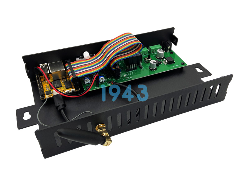
- Functional Testing (FCT): Executing custom-tailored test firmware to validate the electrical and operational integrity of the entire PCBA.

Frequently Asked Questions (FAQ)
Q1: What makes a PCBA NPI service different from standard prototype manufacturing?
Standard prototyping focus solely on assembling a handful of boards as quickly as possible, often overlooking long-term manufacturing flaws. A dedicated NPI service combines fast-turn prototyping with rigorous DFM analysis, testing optimization, and supply chain verification to ensure the design can seamlessly scale to mass production later.
Q2: Why is DFM analysis critical during the initial PCBA design phase?
DFM (Design for Manufacturability) detects layout inconsistencies, component clearance issues, and thermal vulnerabilities before manufacturing begins. Fixing a design flaw in the Gerber files costs a fraction of the price of reworking physically assembled, defective circuit boards.
Q3: How do you ensure high yield and quality for fine-pitch BGA and QFN components?
We utilize automated 3D Solder Paste Inspection (SPI) to guarantee exact paste volume, follow up with precise pick-and-place programming, and employ advanced X-Ray Inspection (AXI) post-reflow to verify internal solder integrity under hidden pads where visual inspection is impossible.
Q4: How are component shortages and obsolescence managed during an NPI project?
Every Bill of Materials (BOM) undergoes a comprehensive lifecycle check. If a component is flagged as obsolete, near End-of-Life (EOL), or faces long lead times, our engineering team identifies and validates pin-to-pin compatible alternatives to present for engineering approval before production starts.
 2026-06-04